LT1055 Precision, High Speed, JFET Input Operational Amplifiers
The LT1055/LT1056 JFET input operational amplifiers combine precision specifications with high speed performance.
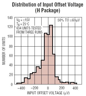
For the first time, 16V/µs slew rate and 6.5MHz gain-bandwidth product are simultaneously achieved with offset voltage of typically 50µV, 1.2µV/°C drift, bias currents of 40pA at 70°C and 500pA at 125°C.
The 150µV maximum offset voltage specification is the best available on any JFET input operational amplifier.
The LT1055 and LT1056 are differentiated by their operating currents. The lower power dissipation LT1055 achieves lower bias and offset currents and offset voltage. The additional power dissipation of the LT1056 permits higher slew rate, bandwidth and faster settling time with a slight sacrifice in DC performance.
The voltage-to-frequency converter shown below is one of the many applications which utilize both the precision and high speed of the LT1055/LT1056.
For a JFET input op amp with 23V/µs guaranteed slew rate, refer to the LT1022 data sheet
产品特点 Features
参数 |
应用
典型应用图 |
LT1055 订购信息和价格参考Package Variations and Pricing
| 器件型号 | 封装 | 引脚 | 温度 | 价格 (以 1 ~ 99 片为批量) | 价格 (以 1000 片为批量) * |
| LT1055CN8 | PDIP | 8 | C | $2.25 | $1.90 |
| LT1055CN8#PBF | PDIP | 8 | C | $2.25 | $1.90 |
| LT1055S8 | SO | 8 | C | $2.67 | $2.35 |
| LT1055S8#PBF | SO | 8 | C | $2.67 | $2.35 |
| LT1055S8#TR | SO | 8 | C | $2.41 | |
| LT1055S8#TRPBF | SO | 8 | C | $2.41 |
LT1055 数据手册及相关资料下载
- 数据手册(英文) : LT1055/LT1056 - Precision, High Speed, JFET Input Operational Amplifiers.PDF
- 应用指南 (英文) : AN10 - Methods for Measuring Op Amp Settling Time.PDF
- 应用指南 (英文) : AN12 - Circuit Techniques for Clock Sources.PDF
- 应用指南 (英文) : AN18 - Power Gain Stages for Monolithic Amplifiers.PDF
- 应用指南 (英文) : AN43 - Bridge Circuits.PDF
- 设计要点 (英文) : DN140 - Updated Operational Amplifier Selection Guide for Optimum Noise Performance.PDF
- 设计要点 (英文) : DN15 - Noise Calculations in Op Amp Circuits.PDF
- 设计要点 (英文) : DN3 - Operational Amplifier Selection Guide for Optimum Noise Performance.PDF
- 设计要点 (英文) : DN6 - Operational Amplifier Selection Guide for Optimum Noise Performance.PDF
- 可靠性数据 : R040 Reliability Data .PDF
- LT Journal : September 2009 - Consider New Precision Amplifiers for Updated Industrial Equipment Designs..PDF
