HMC911LC4B Broadband Analog Time Delay SMT, DC - 24 GHz
The HMC911LC4B is a broadband time delay with 0 to 70 ps continuously adjustable delay range. The delay control is linearly monotonic with respect to the differential delay control voltage (VDCP, VDCN) and the control input has a modulation bandwidth of 1.6 GHz. The device provides a differential output voltage with constant amplitude for single-ended or differential input voltages above the input sensitivity level, while the output voltage swing may be adjusted using the VAC control pin. The HMC911LC4B features internal temperature compensation and bias circuitry to minimize delay variations with temperature. All RF input and outputs of the HMC911LC4B are internally terminated with 50 Ohms to Vcc, and may either be AC or DC coupled. Output pins can be connected directly to a 50 Ohm to Vcc terminated system, while DC blocking capacitors must be used if the terminated system input is 50 Ohms to a DC voltage other than Vcc. The HMC911LC4B is available in RoHS-compliant 4x4 mm SMT package.
技术特性
- Very Wide Bandwidth: DC - 24 GHz
- Continuous Adjustable
Delay Range: 70 ps
- Single-Ended or Differential Operation:
70 ps
- Adjustable Differential Output
Swing: up to 800 mVp-p
- Delay Control Modulation
Bandwidth: 1.6 GHz
- Single Supply: +3.3V
- 24 Lead 4x4mm SMT Package: 16mm²
订购信息 Ordering Information
应用领域 APPLICATION
- Synchronization of Clock & Data
- Transponder Design
- Serial Data Transmission
up to 32 Gbps
- Broadband Test & Measurement
- RF ATE Applications
|
技术指标
Data/
Clock Rate (Gbps/GHz) |
Function |
Rise/Fall Time
(ps) |
Diff. Output Swing (Vp-p) |
Deter-
ministic Jitter (ps) |
DC Power Consumption (mW) |
Vcc Power Supply (Vdc) |
Package |
| 32 / 24 |
Analog Time Delay |
15 / 14 |
0.8 |
6 |
1600 |
+3.3 |
LC4B |
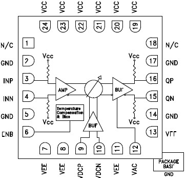
功能框图 Functional Block Diagram
|

