HMC987LP5E 3.3V Low Noise 1:9 Fanout Buffer, DC - 8 GHz
The HMC987LP5E 1-to-9 fanout buffer is designed for low noise clock distribution. It is intended to generate relatively square wave outputs with rise/ fall times < 100 ps. The low skew and jitter outputs of the HMC987LP5E, combined with its fast rise/ fall times, leads to controllable low-noise switching of downstream circuits such as mixers, ADCs/DACs or SERDES devices. The noise floor is particularly important in these applications, when the clocknetwork bandwidth is wide enough to allow squarewave switching. Driven at 2 GHz, outputs of the HMC987LP5E have a noise floor of -166 dBc/Hz, corresponding to a jitter density of 0.6 asec/rtHz - or 50 fs over an 8 GHz bandwidth. The input stage can be driven single-ended or differentially, in a variety of signal formats (CML, LVDS, LVPECL or CMOS), AC or DC coupled. The input stage also features adjustable input impedance. It has 8 LVPECL outputs, and 1 CML output with adjustable swing/power-level in 3 dB steps. Individual output stages may be enabled or disabled for power-savings when not required using either hardware control pins, or under control of a serial-port interface.
技术特性
- Ultra Low Noise Floor: -166 dBc/Hz
@ 2 GHz
- LVPECL, LVDS, CML & CMOS
Compatible Inputs
- Up to 8 Differential or 16 Single-Ended
LVPECL Outputs
- One Adjustable Power CML/RF Output
- Serial or Parallel Control, Hardware
Chip-Enable
- Power-Down Current < 1 uA
- 32 Lead 5x5 mm SMT Package 25 mm²
订购信息 Ordering Information
应用领域 APPLICATION
- SONET, Fibre Channel,
GigE Clock Distribution
- ADC/DAC Clock Distribution
- Low Skew and Jitter Clock
or Data Fanout
- Wireless/Wired Communications
- Level Translation
- High Performance Instrumentation
- Medical Imaging
- Single-Ended to Differential
Conversion
|
技术指标
| Clock Rate (GHz) |
Function |
Input |
Output |
Phase Jitter (12 K to 20 MHz) |
Rise/Fall Time
(ps) |
Channel Skew (ps) |
Power Supply (V) |
| DC - 8 |
1:9 Fanout Buffer |
LVPECL, LVDS, CML, CMOS |
LVPECL |
8 fsRMS |
65 |
3.1 |
3.3 |
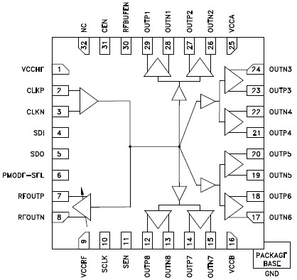
功能框图 Functional Block Diagram
|

