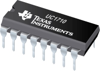
UC1710 辅助大电流 MOSFET 驱动器

The UC1710 family of FET drivers is made with a high-speed Schottky process to interface between low-level control functions and very high-power switching devices-particularly power MOSFET\x92s. These devices accept low-current digital inputs to activate a high-current, totem pole output which can source or sink a minimum of 6A.
Supply voltages for both VIN and VC can independently range from 4.7V to 18V. These devices also feature under-voltage lockout with hysteresis.
The UC1710 is packaged in an 8-pin hermetically sealed dual in-line package for \x9655°C to +125°C operation. The UC2710 and UC3710 are specified for a temperature range of \x9640°C to +85°C and 0°C to +70°C respectively and are available in either an 8-pin plastic dual in-line or a 5-pin, TO-220 package
|
UC1710 |
| No. of Outputs |
1 |
| Driver Configuration |
Inverting, Non-Inverting |
| VCC (Min) (V) |
4.7 |
| VCC (Max) (V) |
18 |
| Peak Output Current (A) |
6 |
| Fall Time (ns) |
8 |
| Prop Delay (ns) |
30 |
| Input Threshold |
CMOS |
| Pin/Package |
8CDIP |
| Approx. Price (US$) |
9.18 | 100u |
| Rating |
Military |
| Operating Temperature Range (C) |
-55 to 125 |
UC1710 特性
- Totem Pole Output with 6A Source/Sink Drive
- 3ns Delay
- 20ns Rise and Fall Time into 2.2nF
- 8ns Rise and Fall Time into 30nF
- 4.7V to 18V Operation
- Inverting and Non-Inverting Outputs
- Under-Voltage Lockout with Hysteresis
- Thermal Shutdown Protection
- MINIDIP and Power Packages
UC1710 芯片订购指南
| 器件 |
状态 |
温度 (oC) |
价格(美元) |
封装 | 引脚 |
封装数量 | 封装载体 |
丝印标记 |
| 5962-0152001QPA |
ACTIVE |
-55 to 125 |
10.03 | 100u |
CDIP (JG) | 8 |
1 | TUBE |
|
| UC1710J |
ACTIVE |
-55 to 125 |
9.18 | 100u |
CDIP (JG) | 8 |
1 | TUBE |
|
| UC1710J883B |
ACTIVE |
-55 to 125 |
10.03 | 100u |
CDIP (JG) | 8 |
1 | TUBE |
|
UC1710 质量与无铅数据
| 器件 |
环保计划* |
铅/焊球涂层 |
MSL 等级/回流焊峰 |
环保信息与无铅 (Pb-free) |
DPPM / MTBF / FIT 率 |
| UC1710J |
TBD |
Call TI |
Call TI |
UC1710J |
UC1710J |
| UC1710J883B |
TBD |
A42 |
N/A for Pkg Type |
UC1710J883B |
UC1710J883B |
| UC1710L |
TBD |
A42 |
N/A for Pkg Type |
UC1710L |
UC1710L |
UC1710 工具与软件
UC1710 应用技术支持与电子电路设计开发资源下载
- UC1710数据资料 dataSheet 下载.PDF
- TI 德州仪器电源管理选型与价格参考 . xls
- U-118 New Driver ICs Optimize High-Speed Power MOSFET Switching Characteristics
- U-137 Practical Considerations in High Performance MOSFET, IGBT and MCT Gate


